Original Article
, Volume: 10( 6)Modification of Distributions of Concentrations Dopants during Overgrowth of Infused-junction and Implanted-junction Rectifiers
- *Correspondence:
- E.L. Pankratov, Nizhny Novgorod State University, 23 Gagarin Avenue, Nizhny Novgorod, 603950, Russia, E-mail: elp2004@mail.ru
Citation: Pankratov EL (2016) Modification of Distributions of Concentrations Dopants during Overgrowth of Infused-junction and Implanted-junction Rectifiers, Nano Science & Nano Technology: An Indian Journal, 10.
Abstract
In this paper we consider influence of overgrowth of doped areas of heterostructures on distributions of concentrations of dopants. The doping has been done by diffusion or ion implantation. Several conditions to increase sharpness of p-n-junctions (single and framework bipolar transistors) have been formulated framework technological process. At the same time we analyzed influence of speed of overgrowth of doped areas and mechanical stress in the considered heterostructures on distribution of concentrations of dopants in the structure.
Keywords
Diffusion-junction heterorectifier; Implanted-junction heterorectifier; Overgrowth of doped area; Analytical approach for modeling.
Introduction
In the present time integration rate of elements of integrated circuits intensively increasing [1-10]. At the same time dimensions of elements of these integrated circuits decreasing and their parameters improved. To increase the integration rate and to decrease dimensions of these elements several approaches have been elaborated and intensively using in the present time [1-10]. Framework this paper we consider a hetero structure. The hetero structure consist of a substrate with known type of conductivity (n or p) and an epitaxial layer. The epitaxial layer has been doped by diffusion or by ion implantation to manufacture another type of conductivity (p or n). Farther we consider overgrowth of the epitaxial layer by an over layer (Figure 1). The overlayer has the same type of conductivity as type of conductivity of the substrate. Main aim of the present paper is analysis of influence of overgrowth of the epitaxial layer on distribution of dopants in the considered heterostructure.

Figure 1: Heterostructure, which consist of a substrate, epitaxial and overlayers.
Method of solution
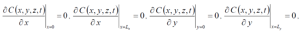
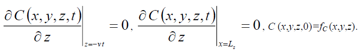
To solve our aim we determine and analyzed spatio-temporal distribution of concentration of dopant in the considered heterostructure. To make the analysis we solve the following boundary problem [1,11-13]
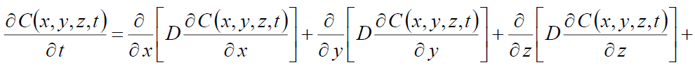
 (1)
(1)

Here C (x,y,z,t) is the spatio-temporal distribution of concentration of dopant; Ω is the atomic volume; symbol  is the surface gradient;
  is the surface concentration of dopant on interface between layers of heterostructure (in this case we consider, that direction Oz is perpendicular to the interface between layers of heterostructure); ? (x,y,z,t) is the chemical potential (reason of accounting of the chemical potential is mismatch-induced stress); D and DS are the diffusion coefficients of volumetric and surface diffusions (reason of the surface diffusions is mismatch- induced stress). Values of these diffusion coefficients depend on properties of materials of heterostructure, temperature and speed of heating and cooling of heterostructure, spatio-temporal distributions of concentrations of dopant and radiation defects. Approximations of the above dependences could be approximated by the following functions [13,14]
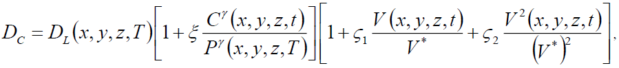
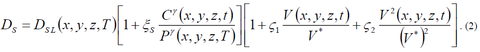
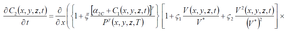
Here DL (x,y,z,T) and DLS (x,y,z,T) are the spatial (due to inhomogeneity of heterostructure) and temperature (due to Arrhenius law) dependences of dopant diffusion coefficients; T is the temperature of annealing; P (x,y,z,T) is the limit of solubility of dopant; parameter γ depends on properties of materials of heterostructure and could be integer in the following interval γ ∈[1,3,14]; V (x,y,z,t) is the spatio-temporal concentration of radiation vacancies; V* is the equilibrium concentration of vacancies. Concentrational dependence of dopant diffusion coefficients has been described in details in [14].
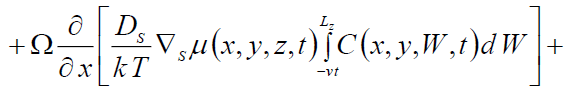
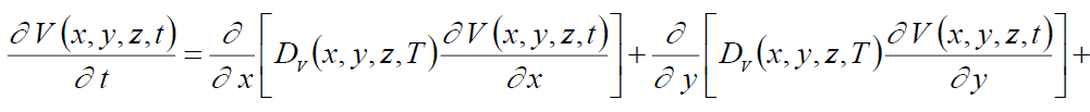
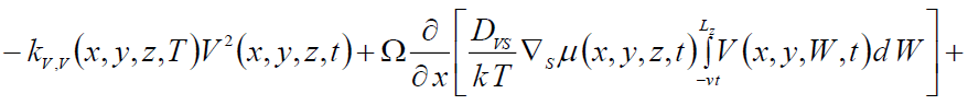
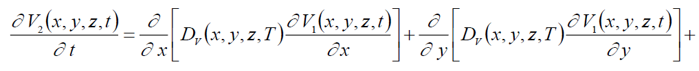
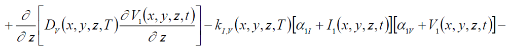
We determine spatio-temporal distributions of concentrations of point defects by solving the following system of equations [1,11-13]


with boundary and initial conditions

I (x,y,z,0)=fI (x,y,z), V (x,y,z,0)=fV (x,y,z). (4)
Here I (x,y,z,t) is the spatio-temporal distribution of concentration of radiation interstitials; I* is the equilibrium concentration interstitials; DI(x,y,z,T), DV(x,y,z,T), DIS(x,y,z, T), DVS(x,y,z,T) are the coefficients of volumetric and surface diffusion; terms V2(x,y, z,t) and I2(x,y,z,t) corresponds to generation divacancies and analogous complexes of interstitials (for example, [13] and appropriate references in this work); kI,V(x,y,z, T), kI,I(x,y,z,T) and kV,V(x,y,z,T) are the parameters of recombination of point defects and generation their complexes; k is the Boltzmann constant.
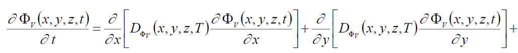
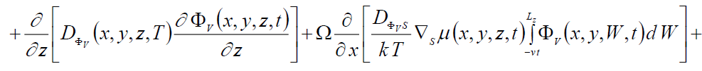
We determine spatio-temporal distributions of concentrations of divacancies ΦV (x, y,z,t) and diinterstitials ΦI (x,y,z,t) by solving the following system of equations [11-13].


with boundary and initial conditions
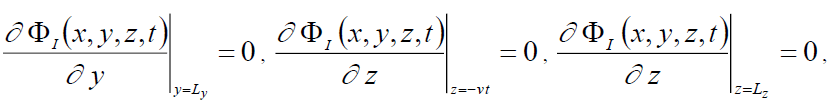
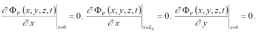


Here  and
and  are the coefficients of volumetric and surface diffusion;
 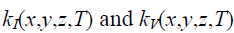 are the parameters of decay of complexes of point defects.
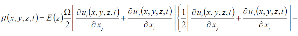
We determine chemical potential ? in the Eq.(1) by the following relation [11]
 (7)
(7)
where E is the tension modulus (Young modulus); 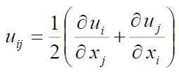 is the deformation tensor; σij is the stress tensor; ui, uj are the components
  and
and of the displacement tensor
 ; xi, xj are the coordinates x, y, z. The relation (3) could be transformed to the following form
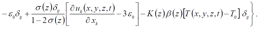
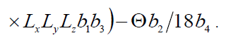
where σ is the Poisson coefficient; ε0=(as-aEL)/aEL is the displacement parameter; as, aEL are the lattice distances of the substrate and the epitaxial layer; K is the modulus of uniform compression; b is the coefficient of thermal expansion; Tr is the equilibrium temperature, which coincide (in our case) with the room temperature.
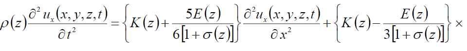
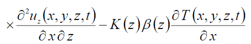
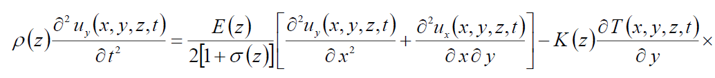
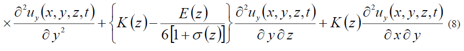
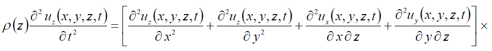
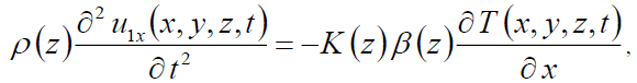
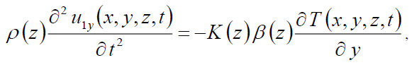
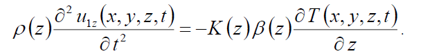
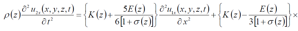
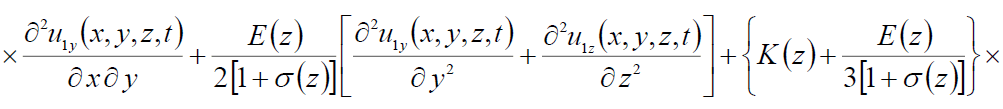
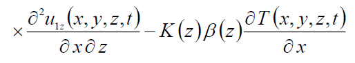
Components of the displacement vector could be determined by solving the following system of equations [15].

where 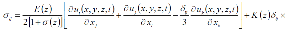
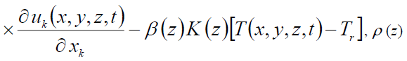 describes the density of materials of heterostructure.
The tensor δij describes the Kronecker symbol. Accounting relation for σij in the previous system of equations last system of equation could be written as:


Systems of conditions for these equations could be written as:

We determine spatio-temporal distribution of concentration of dopant by method of averaging of function corrections [16- 22]. To use the method we re-write equations (1), (3) and (5) with account appropriate initial distributions, i.e. in the following form:


Further we replace required functions in right sides of equations (1a), (3a) and (5a) on their not yet known average values α1ρ. The replacement leads to the following transformation of the above equations:
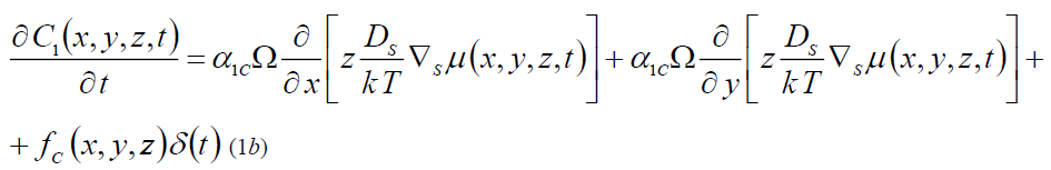
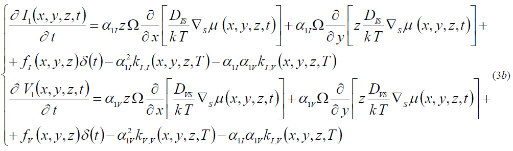
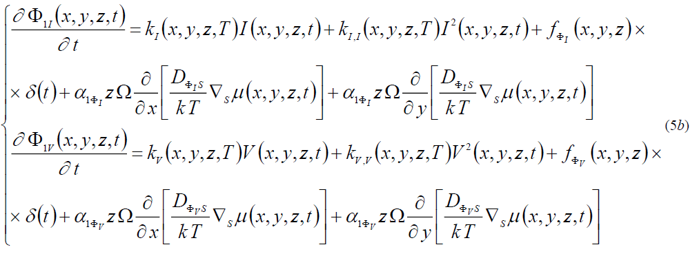
Integration of the left and right sides of equations (1b), (3b) and (5b) give a possibility to obtain relations for the first-order approximations of the considered concentrations in the following final form:


We determined average values of the first-order approximations of the considered concentrations by using the following standard relations [16-22].
 (9)
(9)
Substitution of the relations (1c), (3c) and (5c) into the relation (9) gives a possibility to obtain appropriate average values in the following form:


We calculate approximations of the second and higher orders of concentrations of dopant and radiation defects framework standard iterative procedure of method of averaging of function corrections [16-22]. Framework the procedure to calculate approximations of the n-th order of the above concentrations we replace the functions C(x,y,z,t), I(x,y,z,t), V(x,y,z,t),  in the equations (1a), (3a), (5a) on the sums of the not yet known average values of the considered approximations and approximations of the previous order, i.e.
  After the replacement takes the form:


Integration of left and right sides of Eqs. (1d), (3d) and (5d) gives a possibility to obtain relations for the second-order approximations of the required concentrations of dopant and radiation defects in the following form:


We calculate average values of the second-order approximations of required functions by using the following standard relation [16-21].
Substitution of the relations (1e), (3e), (5e) into the relation (10) gives a possibility to obtain required average values α2ρ


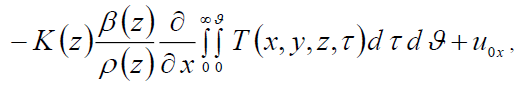
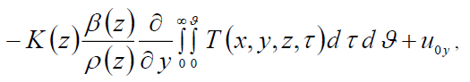
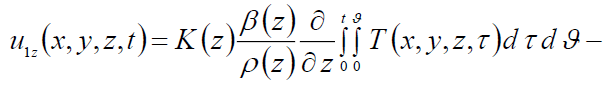
Further we determine solutions of Eqs.(8). In this situation we determine approximation of displacement vector. To determine the first-order approximations of the considered components framework the method of averaging of function corrections we replace the required values on their not yet known average values α1i. The replacement leads to the following result:
Integration of the left and right sides of the previous relations on time t gives a possibility to obtain the required components to the following result:


The second-order, the third-order, … approximations of the displacement vector could be calculated by standard replacement of the required functions in the right sides of the Eqs.(8) on the following sums  [19]. The replacement leads to the following result:


Integration of the left and the right sides of the above equations on time t leads to final relations for components of displacement vector:


Framework this paper all required concentrations (concentrations of dopant and radiation defects) and components of displacement vector have been calculated as the appropriate second-order approximations by using the method of averaging of function corrections. The second-order approximation is usually enough good approximation to obtain qualitative and several quantitative results. All analytical results have been checked by comparison with results of numerical simulation.
Discussion
In this section we analyzed redistribution of dopant with account redistribution of radiation defects (for the ion doping of heterostructure) and interaction of the defects with another defects. If growth rate is small (v t<D1/v), then overlayer will be fully doped by dopant, which was implanted in the epitaxial layer. Framework another limiting case it will be doped nearsurface area of the overlayer only. If dopant diffusion coefficient in the overlayer and in the substrate are smaller, in comparison with the epitaxial layer, and type of conductivity of the overlayer and the substrate is different with type of conductivity of the epitaxial layer, than one can find a bipolar transistor. In this case sharpness of p-n-junctions framework the transistor is higher in comparison with a bipolar transistor in homogenous sample with averaged diffusion coefficient of dopant. At the same time one can find increasing of homogeneity of concentration of dopant (Figure 2). Qualitatively similar results could be obtained for diffusion type of doping. If dopant diffusion coefficient of the overlayer is larger, than in doped epitaxial layer, sharpness of left p-n-junctions became smaller with increasing of homogeneity of concentration of dopant in the overlayer (Figure 3). Qualitatively similar results could be obtained for diffusion type of doping.

Figure 2: Calculated spatial distributions of concentration of implanted dopant in homogenous sample (curve 1) and in heterostructure from Figure 1 (curve 2) after annealing with the same continuance. Interfaces between layers of heterostructure are: a1=Lz/4 and a2=3Lz/4.

Figure 3: Calculated spatial distributions of concentration of implanted dopant in over- and epitaxial layers (curves 1 and 2) and in epitaxial layers only (curves 3 and 4). Increasing of number of curves corresponds to increasing of value of relation D1/D2. Interfaces between layers of heterostructure are: a1=Lz/4 and a2=3Lz/4.
Further we analyzed influence of mismatch-induced stress on distribution of concentration of dopant. We obtain during the analysis, that p-n-junctions, manufactured near interface between layers of heterostructures, have higher sharpness and higher homogeneity of concentration of dopant in enriched area. In directions, which are parallel to the above interface, one can obtain changing of distribution of concentration of dopant due to existing mismatch-induced stress. For example, for ε0<0 the above distribution in directions x and y became more compact (Figure 4). For ε0>0 one can obtain opposite effect (Figure 5). It should be noted, that radiation processing of materials of heterostructure during ion doping of materials gives a possibility to decrease mismatch-induced stress (Figure 6).

Figure 4: Spatial distributions of concentration of dopant in diffusion-junction rectifier after annealing with equal continuance. Curve 1 corresponds to ε0<0. Curve 2 corresponds to ε0=0. Curve 3 corresponds to ε0>0.

Figure 5: Spatial distributions of concentration of dopant in implanted-junction rectifier after annealing with equal continuance. Curve 1 corresponds to ε0<0. Curve 2 corresponds to ε0=0. Curve 3 corresponds to ε0>0.

Figure 6: Normalized dependences of component uz of displacement vector on coordinate uz for epitaxial layers before radiation processing (curve 1) and after radiation processing (curve 2)
Conclusion
In this paper we analyzed influence of overgrowth of doped by diffusion or ion implantation areas of heterostructures on distributions of concentrations of dopants. We determine conditions to increase sharpness if implanted-junction and diffusion- junction rectifiers (single rectifiers and rectifiers framework bipolar transistors). At the same time we analyzed influence of overgrowth rate of doped areas and mismatch-induced stress in the considered heterostructure on distributions of concentrations of dopants.
Acknowledgments
This work is supported by the agreement of August 27, 2013 ? 02.?.49.21.0003 between The Ministry of education and science of the Russian Federation and Lobachevsky State University of Nizhni Novgorod, educational fellowship for scientific research of Government of Russia, educational fellowship for scientific research of Government of Nizhny Novgorod region of Russia and educational fellowship for scientific research of Nizhny Novgorod State University of Architecture and Civil Engineering.
References
- Lachin VI, Savelov NS (2001) Electronics Phoenix, Rostov-na-Donu.
- Fathi D, Forouzandeh B (2009) Accurate analysis of global interconnects in nano-fpgas. Nano 4: 171-176.
- Fathi D, Forouzandeh B, Masoumi N (2009) New enhanced noise analysis in active mixers in nanoscale technologies. Nano 4: 233-238.
- Chachuli SA, Fasyar PNA, Soin N, Karim NM, Yusop N (2014) Pareto ANOVA analysis for CMOS 0.18 µm two -stage Op-amp. Mat Sci Sem Proc 24: 9-14.
- Jung-Hui Tsai, Shao-Yen Chiu, Wen-Shiung Lour, Der-Feng Guo (2009) Semiconductors 43: 971-974.
- Choi JY, Park C (2011) A Thyristor-Only Input ESD Protection Scheme for CMOS RF ICs. Circuits and Systems 2: 170-
- Kumar MJ, Singh TV (2008) Quantum confinement effects in strained silicon MOSFETs MOSFETs. Int J Nanoscience 7: 81-84.
- Sinsermsuksakul P, Hartman K, Kim SB, Heo J, Sun L et al. (2013) Enhancing the efficiency of SnS solar cells via band-offset engineering with a zinc oxysulfide buffer layer. Appl Phys Lett 102: 053901-053905.
- Laajimi R, Masmoudi M (2012) High-Performance CMOS Current Mirrors: Application to Linear Voltage-to-Current Converter Used for Two-Stage Operational Amplifier. Circuits and Systems 3: 311-316.
- Ghorbani A, Ghanaatian A (2012) A Novel High CMRR, Low Power and Low Voltage COS with QFG. Circuits and Systems 3: 263-268.
- Zhang YW, Bower AF (1999) Numerical simulations of island formation in a coherent strained epitaxial thin film system. Journal of the Mechanics and Physics of Solids 47: 2273-2297.
- Fahey PM, Griffin PB, Plummer JD (1989) Point defects and dopant diffusion in silicon. Rev Mod Phys 61: 289.
- Vinetskiy VL, Kholodar' GA. Radiative physics of semiconductors. ("Naukova Dumka", Kiev, 1979, in Russian).
- Gotra Z Yu. Technology of microelectronic devices (Radio and communication, Moscow, 1991).
- Landau LD, Lefshits EM. Theoretical physics. 7 (Theory of elasticity) (Physmatlit, Moscow, 2001, in Russian).
- Sokolov Yu D (1955) About the definition of dynamic forces in the mine lifting. Applied Mechanics 1: 23-35.
- Pankratov EL, Bulaeva EA (2013) Doping of materials during manufacture p-n junctions and bipolar transistors. Analytical approaches to model technological approaches and ways of optimization of distribution of dopants. Reviews in Theoretical Science 1: 58-82.
- Pankratov EL, Bulaeva EA (2015) Materials Science: An Indian Journal. 14: 288-299.
- Pankratov EL, Bulaeva EA (2013) Application of native inhomogeneities to increase com pactness of vertical field-effect transistors. J Comp Theor Nanoscience 10: 888-893.
- Pankratov EL, Bulaeva EA (2014) An approach to manufacture of bipolar transistors in thin film structures. On the method of optimization. Int J Micro-Nano Scale Transp Vol. 4: 17-31.
- Pankratov EL, Bulaeva EA (2014) On the relations between porosity of heterostructured materials and mismatch-induced stress. J Comp Theor Nanoscience 11: 91-101.