Original Article
, Volume: 14( 13)Fabrication and Characterization of Organic Light Emitting Diode Using FTO/Pentacene as Bilayer Anode
- *Correspondence:
- Saikia D, Thin Film Laboratory, Department of Physics, Jagannath Barooah College, Jorhat, Assam, India, 785001, Tel: + 03762320060; E-mail: dhrubajun@gmail.com
Received: September 09, 2016; Accepted: October 13, 2016; Published: October 18, 2016
Citation: Saikia D, Sarma R. Fabrication and Characterization of Organic Light Emitting Diode Using FTO/Pentacene as Bilayer Anode. Mater Sci Ind J. 2016;14(13):103.
Abstract
Pentacene films on FTO surface for affecting the hole injection probability in Organic Light Emitting Diode (OLED) has been investigated. Five kinds of organic light emitting diodes with tris (8-hydroxyquinoline) aluminium (Alq3) as emitting layers were fabricated. It was found that hole injection is directly affected by the different thickness of pentacene films on FTO surface. The OLED device with FTO/pentacene (6 nm) anode shows better device efficiency compared with bare FTO anode and that of other thickness of pentacene films. Enhanced device performance is due to the better surface morphology with large hole mobility, and highest figure of merit (FOM) value of FTO/pentacene (6 nm) bilayer anode combination. In this work N, N’-bis (3-methyl phenyl)-N, N’ (phenyl)-benzidine (TPD) used as hole transport layer and lithium fluoride (LiF) are used as electron injection layer. Our result suggests that the FTO/pentacene (6 nm) anode is an excellent choice to enhanced the hole injection in OLED devices. Here, we obtained maximum value of current and power efficiency are 6.6 Cd/A and 3.4 lm/W respectively.
Keywords
Optoelectronics; Pentacene; Flourine doped tin oxide (FTO); FOM; Hole injection
Introduction
Small molecule Organic Light Emitting Diodes (SOLEDs) are great interest due to their great applicability in flat panel display and solid state lighting. Tin-doped indium oxide (ITO) with electrical conductivity and visible range transparency of 3 × 10³ S/cm to 5 × 10³ S/cm and 85% to 90% respectively, is currently the most widely used OLED anode material. However, rising in costs and other limitations present challenges for next generation optoelectronic devices [1,2]. Also in the case of ITO anode the diffusion of indium into the organic layers during device operation, which was found to be correlated with the decay of device performance [3].
In addition, indium tin oxide (ITO) possesses a relatively lower work function (4.4 eV to 4.9 eV) and therefore several approaches have been employed to overcome relatively high hole injection barrier between the ITO and the organic emitting layers by inserting buffer layer; transition metal oxide [4,5], small organic molecule [6] and conducting polymers [7,8]. Because the presence of such injection layer enhanced the hole injection into the organic layers and improves the surface roughness of ITO anode system which directly affect the device performance including its turn on voltage. Inorganic insulating buffer layer such as LiF [9,10], Al2O3 [11], SiO2 [12], MoO3 [13] were reported in the literature. Zhang et al. [14] calculated the J-V characteristics of OLEDs having a uniform buffer layer based on the WKB approximation. Lu and Yokoyama [15] reported hole block effect due to the insertion of Ta2O5 and HfO2 buffer layers whereas other reports showed apparent enhancement of hole injection with the insertion of various buffer layers such as LiF [10], SiO2 [12], WO2.5 [16] etc. Recently, Reddy et al. [17,18] reported some newly bipolar solution process dihydroacridine derivatives for highly efficient organic light emitting diode.
The Vanadium pentoxide (V2O5) has also been used as a modification of ITO anode to enhanced hole injection [19,20] due to its suitable value of work function. Zhang and Choy [21] investigated Au/V2O5 films on ITO as composite anodes for the hole injection in OLEDs with maximum current efficiency 3.5 Cd/A. Thus, all the maximum reports are found to be based on ITO. On the other hand, Fluorine-doped Tin Oxide (FTO) though being cost effective and more stable to oxidation than the ITO; it is not widely used to fabricate OLEDs because of its less transparency than ITO. There are few published reports that indium tends to diffuse into the emissive layer under device operation, which may in turn influence the quantum efficiency and lifetimes of OLEDs. Similarly, the chemical composition, as well as the work function of FTO, was independent of the cleaning methods employed.
It has also some merit side like it is not classified as a substance dangerous for carriage or supply and not hazardous to the environment. Also for the FTO anode, no risk or safety phrases are necessary. On the other hand, although pentacene has high hole mobility but till now it is not used as a buffer layer in the society of OLED. So, in this work we focus our attention on this specific bilayer combination to increase both the current and power efficiency for the first time on FTO surface which also acts as a barrier for the metallic diffusion into the organic layer. For this purpose, we take the help of thickness variation method in which a series of pentacene films of different thicknesses were deposited on FTO anode and we report that pentacene thin films acting as hole injection layer (HIL) can improve the current efficiency of OLEDs based on Alq3 as the emission layer and finally we report a better OLED device with maximum current efficiency of 6.6 Cd/A with this bilayer anode combination at optimized thickness of pentacene. In this paper, OLED were characterized in terms of their current efficiency (g) and power efficiency (h).
Experimental Details
All devices were fabricated on FTO-coated glass and thermally deposited AL was used as a cathode. The FTO glass was cleaned in an ultrasonic bath of acetone and isopropanol for 15 minutes and the deposition was carried out at a pressure less than 5 × 10⁻⁵ torr. All the organic and inorganic layers were evaporated at the deposition rate higher than 10 Å/sec. The devices have an active emissive area of 8 × 8 mm2. All the devices were fabricated by using Thermal Vacuum Evaporation Unit and the corresponding film thickness were recorded by thickness monitor (Model DTM-10). The sheet resistance of the different films was recorded by using four-probe resistivity measurement. The current-voltage-luminance characteristics of the fabricated OLEDs were measured by digitally controlled source-meter unit (SMU) and luminance meter unit under dark room condition and the transmittance spectra of the different bilayer FTO/pentacene films are recorded by UV-Double beam spectrophotometer set up. All tests are performed in air at room temperature under dark room condition without any encapsulation and all materials are purchased from Sigma-Aldrich and used without further purification. A schematic representation and energy band diagram is shown by following Figure 1 and Figure 2 respectively.

Figure 1: Schematic presentation of OLED.

Figure 2: Energy band diagram of OLED.
Result and Discussion
We have fabricated the standard OLED samples using pentacene as hole injection layer (HIL), N, N’-bis (3-methyle phenyl)- N, N’(phenyl)- benzidine (TPD), Tris (8-hydroxy quinolinato) aluminium (Alq3) and lithium fluorides (LiF) are used as hole transport layer, light emitting layer, and electron injection layer respectively and compared the J-V-L characteristics of OLEDs with different thickness of HIL and that of HIL free OLED. Without LiF (EIL) layer, electron injection from Al cathode into Alq3 is difficult. Because the dissociation of alkali halide into the organic layer improve the electron injection process. The structures of the bottom emitting OLEDs used in this study are:
Device 1. FTO/Pentacene (0 nm)/TPD (45 nm)/Alq3 (56 nm)/LiF (5 nm)/Al (100 nm)
Device 2. FTO/pentacene (1 nm)/TPD (45 nm)/Alq3 (56 nm)/LiF (5 nm)/Al (100 nm)
Device 3. FTO/pentacene (4 nm)/TPD (45 nm)/Alq3 (56 nm)/LiF (5 nm)/Al (100 nm)
Device 4. FTO/pentacene (6 nm)/TPD (45 nm)/Alq3 (56 nm)/LiF (5 nm)/Al (100 nm)
Device 5. FTO/pentacene (10 nm)/TPD (45 nm)/Alq3 (56 nm)/LiF (5 nm)/Al (100 nm)
For proper efficiency in an organic semiconductor requires not only balanced injection but of also similar mobility values for holes and electrons. This is accomplished by incorporating an electron transport layer (ETL), in which conduction is dominated by electrons and a separate hole transport layer (HTL), in which conduction is dominated by holes. This configuration allows independent optimization of the injection and transport characteristics using respectively, properly selected electrodes and transport materials. Characteristics curve for OLEDs are given below:
In Figure 3a, in which device 4 gives the better luminance along with high current efficiency (g) as shown in Figure 3b. Similarly, the variation of current efficiency vs applied voltage is shown in Figure 3d in which device 4 achieve the highest performance. The behavior of each device is discussed here. The device with the single FTO anode shows poor hole injection and the luminance is substantially lower than the other pentacene based OLED devices at the same voltages. But however, among the four-bilayer anode OLED device, device 4 shows a maximum current efficiency of 6.6 Cd/A due to the peculiar behavior of pentacene film at 6 nm thickness i.e. optimized transmittance and surface resistance property within tunneling region.

Figure 3: a) Graph of luminance vs current density and transmittance vs wavelength. b) Graph between current efficiency and current density. c) Graph of power efficiency (η) and voltage (V). d) Graph between current efficiency and voltage.
From the Table 1, it is clear that both the electrical and optical properties are decreased with the increasing thickness of the buffer layer. In fact, at the thickness of 10 nm organic film the average transmittance of bilayer film (within 500 nm to 600 nm) is larger than 80%, which is greater than the inorganic metal oxide buffer layer OLED device [21] as shown in Figure 3a. Therefore, we can say that this inorganic-organic bilayer anode film has the more advantage as transparent performance than the inorganic-inorganic based bilayer anode device. We also calculated the figure of merit (FOM) values for FTO and pentacene modified OLED devices. This can be calculated with the help of surface resistance and optical transmittance observation.
| Anode combination | Surface resistancea(Ω/square) | Transmittance (%) | Figure ofmerit (Ω-1) | Current efficiency (cd/A) | Device Turn-on voltage(V) |
|---|---|---|---|---|---|
| FTO/Pentacene (0 nm) | 23.82 | 85.35% | 8.26 × 10⁻³ | 3.7 | 6.5 |
| FTO/pentacene (1 nm) | 23.19 | 84.81% | 8.30 × 10⁻³ | 4.3 | 6.4 |
| FTO/pentacene (4 nm) | 21.86 | 84.35% | 8.34 × 10⁻³ | 4.8 | 6.1 |
| FTO/pentacene (6 nm) | 20.04 | 83.65% | 8.37 × 10⁻³ | 6.6 | 5.8 |
| FTO/pentacene (10 nm) | 17.61 | 82.45% | 8.24 × 10⁻³ | 1.8 | 7.2 |
aSurface resistance fluctuate within a range of ± 0.06 Ω/square.
Table 1: Summary of the surface property of anode combination at different thickness.
Based on this observation, we analyzed the figure of merit (FOM) which is a function of sheet resistance and optical transmittance. This is an important parameter for study the performance of transparent conducting oxide (TCO) films. The FOM is defined as FOM=T10/Rs, where T is the optical transmittance and Rs is the sheet resistance [22]. Table 1 shows the anode surface resistivity of the pentacene modified FTO with a varied thickness from 1 nm to 10 nm with their FOM values. Since the higher value of the figure of merit indicates the high quality of transparent conducting oxide films. So the FTO surface with a 6 nm thick pentacene buffer layer will clearly give better performance as a transparent conducting oxide than that of the single layer FTO film. The two efficiencies i.e., power efficiency (η) and current efficiency (γ) are not independent. Assuming a Lambertian emission pattern [23].
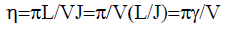 (1)
(1)
where L is measured normal to the emitting surface and V is the applied voltage. While γ depends on the optical coupling and the internal quantum efficiencies [24]. It is fairly constant or weakly varying over a large range of J. On the other hand, h is clearly bias dependent and inversely proportional to V.
To investigate the influence of the pentacene film on the FTO substrate, the surface resistivity of FTO and pentacene modified substrate were measured by four probe resistivity measurement. The results revealed that there are optimum thicknesses of buffer layer at which the OLED current efficiency can be achieved. In this case, the optimum thickness of 6 nm pentacene buffer layer has resulted in 1.78 times enhancement in current efficiency. Too thin (1 nm) or too thick (10 nm) of pentacene buffer layer does not help in improving the current efficiency.
Table 1 shows the anode surface resistivity of the pentacene modified FTO with a varied thickness from 1 nm to 10 nm. Lower sheet resistance means holes would need less energy to overcome the barrier to inject into the organic layer according to the thermionic emission mechanism which would normally result in less threshold voltage, higher current and power efficiency within tunneling region. In our work, current efficiency gets the highest improvement at the optimal thickness (6 nm) of pentacene buffer layer where the hole and electron injection reach the maximum balance point. But after the critical thickness device performance is reduced due to more reduction of tunneling effect. This means that although surface properties are reduced with increasing thickness of buffer layer but there is a more balancing of charge carrier is occur because of which device efficiency is optimized along with both luminance and current density value. As for the improvement of power efficiency, it is related to the energy consumption of hole injection. Due to the smooth surface property, less energy is consumed at the anode/HTL interface. This effect gets an optimal balance at the thickness of 6 nm of Pentacene buffer layer which exhibits the highest improvement of power efficiency (3.40 lm/W) in our device configuration as shown in Figure 3c. Relation between the different thickness of pentacene film and the corresponding turn-on voltage is shown by the following Figure 4.:

Figure 4: Variation of turn-on voltage vs buffer layer thickness.
From this graph, we conclude that the thickness of the buffer layer on the FTO substrate has a direct impact on the injection of charge carrier (i.e., hole) into the organic layers. In our work, we obtain the lowest turn-on voltage is 5.8 V. The initial decreasing of the turn-on voltage is caused by a decrease in the effective surface resistance and the barrier energy. This situation is linked with the energy levels of buffer layer and HTL at their interface which is modulated by the internal electric field. This internal field modulation mainly causes for the reduction of device turn on voltage. But after the optimal thickness any addition of buffer layer thickness causes conduction loss increase instead of a further reduction in turn-on voltage. This is due to the relatively weak modulation by image-force lowering of the buffer layer [25] after critical thickness.
For the surface morphology purpose, we take the FE-SEM images of both the single and bilayer FTO anode as shown in Figure 5a and 5b. From the study of FE-SEM images it can be concluded that the surface of bilayer anode became smoother compared to the single anode due to the presence of organic layer. Therefore, this organic buffer layer provides better organic-organic contact compared with that of the inorganic-organic contact with the HTL layer, because of which we get the better device efficiency when proper bias is applied within the tunneling region. This is an important reason for reducing the contact resistance and increases the hole injection.

Figure 5: a) FE-SEM image of FTO. b) FE-SEM images of bilayer FTO/Pentacene anode film.
Conclusion
Thin pentacene film deposited by thermal vacuum deposition has been employed as a buffer layer on OLED anode. Current efficiency and power efficiency of the device with an optimal thickness of 6 nm high-quality pentacene buffer layer were simultaneously increased compared with bare FTO anode OLED. The improved current efficiency is attributed to a balanced contribution of thermionic emission of charge carrier in the presence of an optimal thickness of pentacene buffer layer which are proved by transmittance spectra and surface resistivity measurement. The improved power efficiency is due to the balanced of energy consumption. The device with FTO/pentacene (6 nm) as anode provides a better charge balance which makes the current efficiency (6.6 Cd/A) 1.78 times higher than that of the FTO OLED (3.7 Cd/A).
References
- Schlatmann AR, FloetWD, Hilberer A, et al. Indium contamination from the indium–tin–oxide electrode in polymer light?emitting diodes. Appl Phys Lett. 1996;69(12):1764.
- Jansseune T. Compound Semiconductor Magazine. September 2003.
- Lee ST, Gao ZQ, Hung LS.Metal diffusion from electrodes in organic light-emitting diodes. Appl Phys Lett. 1999;75(10):1404.
- Hu WP, Manabe K, Furukawa T, et al.Lowering of operational voltage of organic electroluminescent devices by coating indium-tin-oxide electrodes with a thin CuOx layer.Appl Phys Lett. 2002;80:2640.
- Kabra D, Lu LP, Song MH, et al. Efficient single-layer polymer light-emitting diodes. Adv Mater.2010;22(29):3194-8.
- Vasilopoulou M, Palilis LC, Georgiadou DG, et al.Barrierless hole injection through sub-bandgap occupied states in organic light emitting diodes using substoichiometricMoOx anode interfacial layer. Appl Phys Lett.2012;100:013311.
- Hong IH, Lee MW, Koo YM, et al. Effective hole injection of organic light-emitting diodes by introducing buckminsterfullerene on the indium tin oxide anode. Appl Phys Lett.2005;87(6):063502.
- Kim TY, Suh M,Kwon SJ, et al. Poly(3,4-ethylenedioxythiophene) Derived from Poly(ionic liquid) for the Use as Hole-Injecting Material in Organic Light-Emitting Diodes. Macromol Rapid Commun. 2009;30(17):1477-82.
- Huang LS, Tang CW, Mason MG. Enhanced electron injection in organic electroluminescence devices using an Al/LiF electrode. Appl Phys Lett.1997;70(2):152.
- Mori T,Fujikawa H, Tokito S, et al. Electronic structure of 8-hydroxyquinoline aluminum/LiF/Al interface for organic electroluminescent device studied by ultraviolet photoelectron spectroscopy. Appl Phys Lett. 1998;73(19):2763.
- Zhang ST,Zhou YC, Zhou JM, et al. Role of hole playing in improving performance of organic light-emitting devices with an Al2O3 layer inserted at the cathode-organic interface. Appl Phys Lett. 2006;89(4):043502.
- Deng ZB, Ding XM, Lee ST, et al. Gambling Enhanced brightness and efficiency in organic electroluminescent devices using SiO2 buffer layers. Appl Phys Lett. 1999;74(15):2227.
- Meyer J, Shu A,Kröger M, et al.Effect of contamination on the electronic structure and hole-injection properties of MoO3/organic semiconductor interfaces. Appl Phys Lett. 2010;96(13):133308.
- Zhang ST, Ding XM, Zhao JM, et al. Buffer-layer-induced barrier reduction: Role of tunneling in organic light-emitting devices. Appl Phys Lett. 2004;84(3):425.
- Lu HT, Yokoyama M.Enhanced emission in organic light-emitting diodes using Ta2O5 buffer layers. Solid State Electron.2003;47(8):1409-12.
- VasilopoulouM, PapadimitropoulosG, PalilisL, et al. High performance organic light emitting diodes using substoichiometric tungsten oxide as efficient hole injection layer. Org Electron.2012;13(5):796.
- Reddy SS, SreeGV, Gunasekar K, et al. Highly efficient bipolar deep-blue fluorescent emitters for solution-processed non-doped organic light-emitting diodes based on 9,9-Dimethyl-9,10-dihydroacridine/Phenanthroimadazolederivatives. Adv Opt Mater. 2016;4(8):1236-46.
- Reddy SS, Cho W, SreeGV, et al. Multi-functional highly efficient bipolar 9,9-dimethyl-9,10-dihydroacridine/imidazole-based materials for solution-processed organic light-emitting diode applications. Dyes Pigm. 2016;134:315-24.
- Bruner EL, Koch N, Span AR, et al. Controlling the work function of indium tin oxide: differentiating dipolar from local surface effects. J AmerChemSoc. 2002;124(13):3192-3.
- Zhu XL, Sun JX, Peng HJ, et al. Vanadium pentoxide modified polycrystalline silicon anode for active-matrix organic light-emitting diodes. Appl Phys Lett.2005;87(15):153508.
- Zhang HM, Choy WCH. Indium tin oxide modified by Au and vanadium pentoxide as an efficient anode for organic light-emitting devices. IEEE TransactElectr Dev. 2008;55(9):2517-20.
- Hu WP, Manabe K, Furukawa T, et al.Lowering of operational voltage of organic electroluminescent devices by coating indium-tin-oxide electrodes with a thin CuOx layer. Appl Phys Lett. 2002;80(15):2640.
- Haacke G. New figure of merit for transparent conductors. J Appl Phys.1976;47(9):4086.
- Kim JS, Ho PKH, GreenhamNC, et al. Electroluminescence emission pattern of organic light-emitting diodes: Implications for device efficiency calculations. J Appl Phys. 2000;88(2):1073.
- ArkhipovVI, Bassler H. Tandem injection of charge carriers across a metal-dielectric interface. Appl Phys Lett. 2000;77(17):2758-60.