Research
, Volume: 15( 2) DOI: 2021;19(6):158A Novel Route Synthesis of Zinc Tellurium Thin Films and its Characterization
Kishan C Rathod*
Department of Chemistry, The New College, Kolhapur, India
*Corresponding author:
Kishan C Rathod
Department of Chemistry, The New College, Kolhapur, India
Tel: 9067868043
E-mail: kishanchandurathod@gmail.com
Received: August 17, 2021; Accepted: August 31, 2017; Published: September 07, 2017
Citation: Kishan C Rathod. A Novel Route Synthesis of Zinc Tellurium Thin Films and its Characterization. Mat Sci Ind J. 2021;19(6):158
Abstract
Crystalline zinc telluride thin films have been deposited on non-conducting glass substrates using triethanolamine chemical bath deposition method. The film samples were characterization by X-ray diffraction scanning electron microscopy optical spectroscopy and thermoelectric techniques. The Crystalline phase of the deposited sample was of orthorhombic type. The optical band gap energy of the sample was found to be 2.15 eV. The electrical conductivity of the film sample was found to be in the order of 10-8 (â?¦ cm)-1 .
Keywords: CBD;X-raydiffraction
Introduction
Now a day thin film is one of the most important technologies that contributed to the development of semiconductor. Thin film is layer or several layer of certain atoms whose thickness is within nanometer to two microns resulting from the condition of atoms or molecule that possess unique properties that differ from whether they are thick particle possessing physical and chemical properties with the appropriate microstructures. There is another type of the thin film, called a thick film, which is identifier as a small dimensional substance formed with a large accumulation of cluster ion.
Thin films deposition depends on several factors including ground temperature, pH and concentration of the solution, and speed of the rotation [1]. Research focused today on manufacturing low cost thin films with high efficiency and because of their wide application in several field such as electric devices in the form of resistors, transistor, capacitors and other is mainly for the manufacture of solar and photovoltaic cells, electro optics detectors within specific spectral ranges for various application.
The semiconductor ZnTe thin film is one of the most important semiconductors because of its optical and electrical properties. It has a rather large direct energy band gap of 2 to 2.3 eV which make it suitable in many uses including light emitting diode, terahertz devices, electric devices, and photosensor.
The energy gap for the semiconductor ZnTe depends on a group of factors, including preparation method, temperature, solution concentration, pH of the solution, and speed of the rotation reaction mixture and the compounds used as sources for the zinc and tellurium elements. The ZnTe is made up of two elements Zinc and tellurium and interaction requires high temperature to form a ZnTe thin film. In the novel synthesis of Zinc telluride thin films on non –conducting glass substrate from aqueous alkaline medium. We report here the synthesis of Zinc telluride thin films using chemical bath deposition method and characterization for their optical, structural, surface morphology, electrical properties and photoelectrical performance.
Materials and Methods
Experimental details
In actual experimentation, 10 mL (1 M) zinc sulphate solution was taken in 250 mL beaker; 5 ml TEA, 10 mL liquor ammonia, and 10 mL (1 M) sodium telenosulphate was added in the reaction bath at room temperature pH of the reaction mixture was found to be 10 ± 5. The beaker was kept in oil bath, the non-conducting glass substrate were mounted vertically on a specially designed substrate holder and rotated in the reaction mixture with a speed of 65 ± 2 rpm. The temperature of bath was then allowed to increase slowly up to 369 K. After 7 hours 50 minute the slides were removed, washed with deionized water several times, dried naturally and preserved in desiccator.
Sample Characterizations
X-ray diffraction of zinc telluride thin films was carried out in the range of the diffraction angle 10-1000 with CuKa1 radiation using Philips PW–1710 diffract meter (l=1.54056 Å). The electrical conductivity of zinc telluride thin films was measured using a ‘dc’ two-probe method. A quick drying silver paste was applied at the end of the film for ohmic contact purpose. The layer thickness of the film was measured by weight difference method. The optical absorbance measurements were made in the wavelength range 400-1200 nm by using a Hitachi-330 (Japan) UV–visible NIR, double beam spectrophotometer at room temperature, uncoated glass substrate placing in the reference beam made substrate correction. A 250 MK-III StereoScon (USA) scanning electron microscope (SEM) was used for the microscopic observations.
Results and discussion
Kinetics and growth mechanism
In the reaction bath Zn+2 ions are complexed with TEA in the form of water-soluble Zn-TEA complexed and thus control Zn+2 concentration. The dissociation of sodiumtelenosulfate as well as Zn-TEA complex in alkaline medium takes place.
At low temperature kinetic energy is lower and avoids the precipitation. Thermal decomposition of metastable complex releases metal ions while sodiumtelenosulphate hydrolyzes in alkaline solution to yield Te-2 ions transferred to an ice bath at 278 K temperature. The pH of the resulting solution was found to be 11.80 ± 0.05. The temperature of the solution was then allowed to rise slowly to 293K. The stainless-steel
plate was subsequently removed from the beaker after 6 h of deposition (Table 1).
TABLE 1. Structural parameters of the synthesized metal oxide nanomaterials.
| Film | d values (Å) | hkl planes | Grain size (XRD)(Å ) | Cell parameter,a (Å) | |
|---|---|---|---|---|---|
| ASTM | Observed | ||||
| ZnTe | 2.869 | 2.861 | 200 | 186 | |
| 2.564 | 2.561 | 321 | |||
| 2.505 | 2.499 | 302 | a=4.7244 | ||
| 1.9189 | 1.916 | 22 | b=8796 | ||
| 1.6244 | 1.62 | 311 | c=5.0100 | ||
| 1.4827 | 1.487 | 40 | |||
| 1.3647 | 1.367 | 400 | |||
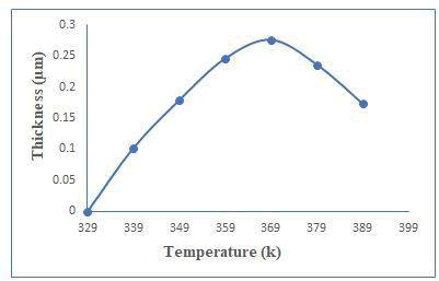
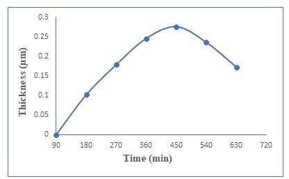
The presence of induction period suggests that ion-by-ion growth mechanism instead of cluster by cluster. Figure 1(a) shows the thickness against deposition temperature. Zinc telluride thin films have been well deposited at 450 minutes with 0.276 μm thicknesses. The thickness was measured every 90 minutes and plotted against time as shown in Figure 1(b). Rotation speed was 65 ± 2 rpm to maintained constant deposited zinc telluride thin films [2]. The optimum conditions like for temperature and time are at 369 k and 450 minutes respectively (Figure 1a and 1b).
X-ray diffraction studies
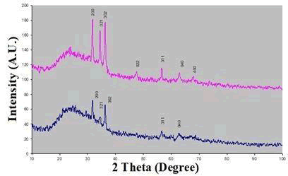
X-ray diffraction studied by the pattern of ‘as deposited’ and annealed Zinc telluride thin films, are shown in Figure 2. The X-ray diffraction pattern of the ‘annealed’ sample shows high peak intensity, due to high crystallinity. The observed d-value correspond to 2.861 phase of Zinc telluride and are indexed according to Orthorhombic structure (JCPDS -822152). The indices are shown above the reflections in the figure. The XRD pattern shows the highest intensity reflection peak at d=2.861Å (200), Along with (321) plane, (302), (022), (311), (040), (400), peaks are also observed (Figure 2).
Morphological characterization
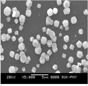
A study of surface morphology of thin film was done under scanning electron microscopy, 250 MK III stereos can Cambridge, UK. Scanning electron microscopy is an excellent method to study morphology of the sample. The scanning electron micrograph of the ‘as deposited’ thin film is shown in Figure 3. The film shows uniform grains and attached the substrate well [3]. The distribution of nodular, spherical grains of almost similar size is observed. Most of grains separated with each other. The presence of fine background is an indication of one step growth by multiple nucleations (Figure 3).
Optical characterization
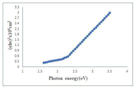
The absorption spectrum of sample was recorded at room temperature in the wavelength range of 400-1200 nm. The value of absorption coefficients depends upon radiation energy as well as composition of thin films [4]. It is probably due to increase in the grain size leading to reduction in the density of grain boundary trapping centers and the change in the colour form white to gray white. This shift indicates decrease in band gap of the sample and the following classical relation for near absorption edge in a semiconductor (Figure 4).
Electrical characterization
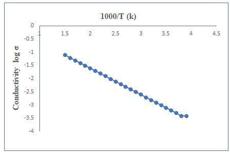
The electrical measurements were carried out using two-probe method in the temperature range 300-525 K. At room temperature the specific conductance was found to be into order of 10-8 (?cm)-1. It is observed that the conductivity behavior of the film. A plot of log (conductivity) versus inverse absolute temperature for the cooling and heating curve is shown in Figure 5. A plot showing the straight-line nature indicates the presence of only one type of conduction mechanism. The activation energy is calculated using exponential form of Arrhenius relation (Figure 5) [5].
Conclusion
Binary zinc tellurium thin films have been grown on to non-conducting glass substrates by using chemical bath deposition method. The optical absorption studies showed zinc telluride sample have direct band gap of 2.15 eV. X-ray diffraction studies zinc telluride thin film is orthorhombic phase. Temperature dependence of electrical conductivity shows that p-type semiconducting nature of films. The material shows promising photo-response when tested in iodine-iodine electrolyte. The photo electrochemical cell was found to be 1.13% efficiency.
References
- Abbasm M, Shorb NA, Jehangir K, et Physicsl properties of ZnTe semiconductor thin films prepared by high vaccum resistive system.
- Mater Sci. 2018;36:364-69.
- Abegund OO, Akinlabi ET, Oladijo OP, et Overview of thin film deposition techniques AIMS. Mater Sci. 2019;6(2):174-79.
- Promnopas W, Thongtem T, Thongtem ZnTe semiconductor polymer gel composited electrolyte for conversion of solar energy. J
- Nanomater. 2014;1-6.
